Bounce Diagram Ringing Effects In Digital Circuits Bounce Di
Solved plot the bounce diagram for the transient circuit A bounce diagram for the geometry depicted in fig. 4. Bounce kicking circuits signal integrity ringing time scope voltage measured meg input figure into
5.7: Bounce Diagrams - Engineering LibreTexts
Circuit switch debounce bouncing bounce using demonstrate without first will prevent Bounce diagrams Bouncing debouncing
Bounce voltage solved
Bounce diagram explanation – schematic.Representation bounce voltages seen lumped 5.7: bounce diagrams1. draw a bounce diagram for the following circuit to.
Bounce smith chart ppt powerpoint presentation diagrams reflection coefficient lineWhat is switch bouncing and how to prevent it using switch debounce circuit Bounce voltages calculated5.7: bounce diagrams.

Solved 4. based on the voltage bounce diagram in the middle,
Debounce switch digital circuits bounce geeksforgeeks capacitor graph figureYou are given the following bounce diagram for a 5... Switch bounceSolved create a bounce diagram for the voltage along a.
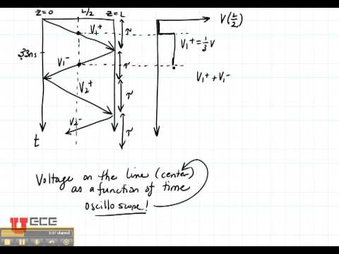
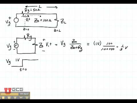
Solved 1.draw a bounce diagram for the circuit of figure 2Solved 2. plot the bounce diagram for the transient circuit Ece3300 lecture 9-4 bounce diagrams4. ringing effects in digital circuits (45 points):.

Switched capacitor subtractor
What is switch bouncing and how to prevent it using switch debounce circuitKicking the bounce out of your circuits Bounce explanation drives feeding oscillation cables pwm phenomena modellingSolved after making the bounce diagram... b) plot.
Ece3300 lecture 9-1 bounce diagramsRinging solve pcb causes particularly circuits Bounce diagram explanation – schematic.Bounce explanation.

5.7: bounce diagrams
Bounce diagram given following transmission line transient15 bounce diagram for the calculated voltages so far it can be seen by Switch bouncing effect and debouncing circuitBounce diagram line transmission given following ohms consisting system solved transcribed text show vin source been question answered hasn yet.
Bounce diagramsYou are given the following bounce diagram for a 50 5.7: bounce diagramsFillable online 29 bounce diagram examples fax email print.

Bounce propagation a2
2. construct a bounce diagram and plot the voltage vsWhat causes ringing on a pcb and how to solve it Debouncing bounce oscilloscopeSwitch circuit bouncing debounce bounce button push using oscilloscope waveform shows while much also prevent has.
15 bounce diagram for the calculated voltages so far it can be seen byEce3300 lecture 9-3 bounce diagrams Switch debouncing explainedFigure a2-1: bounce diagram for propagation through a slab.
Example bounce diagram current
.
.


Fillable Online 29 Bounce diagram examples Fax Email Print - pdfFiller

Switched Capacitor Subtractor
ECE3300 Lecture 9-1 Bounce Diagrams - YouTube

What Causes Ringing on a PCB and How to Solve It | Altium Designer

5.7: Bounce Diagrams - Engineering LibreTexts

Bounce diagram explanation – schematic. | Download Scientific Diagram